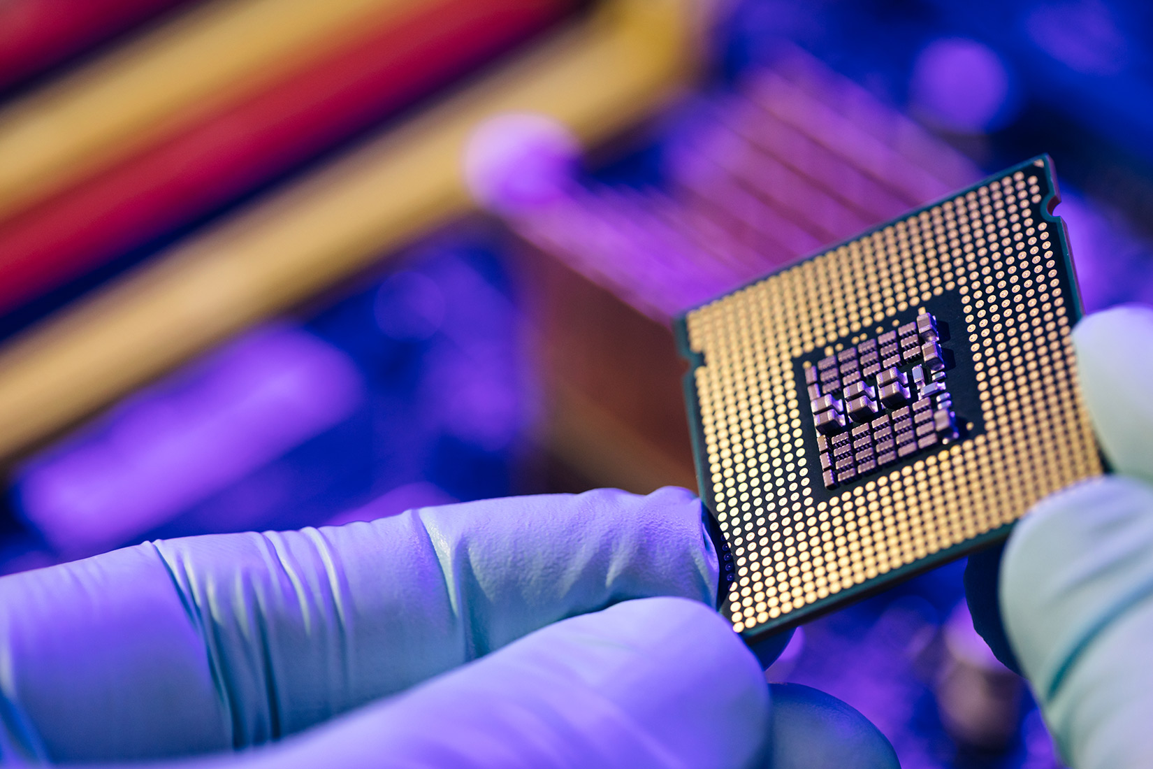
For many years, microelectronic packages consisted of only a few layers. Now, as 3D packaging becomes a common method for bringing more functionality to smaller devices, die inspection systems have to penetrate many more layers – including overmolds, metallization and dielectric layers below a die, multiple stacked dies, or all of these. As manufacturers incorporate smaller features such as Cu pillars into their advanced package designs, they need to solve the challenge of getting clear incspection images through these multiple package layers.
Acoustic reflections from deeper layers within a stacked die package are weaker than reflections from shallower layers. This is the result of basic physics, as the energy of the signal is reduced by reflections from each successive stacked die layer. SDI technology, exclusively from Sonix, allows customers to set a gain profile that provides clear imaging at each layer in the stacked die package without requiring multiple scans and without obscuring defects in shallow images through oversaturation.
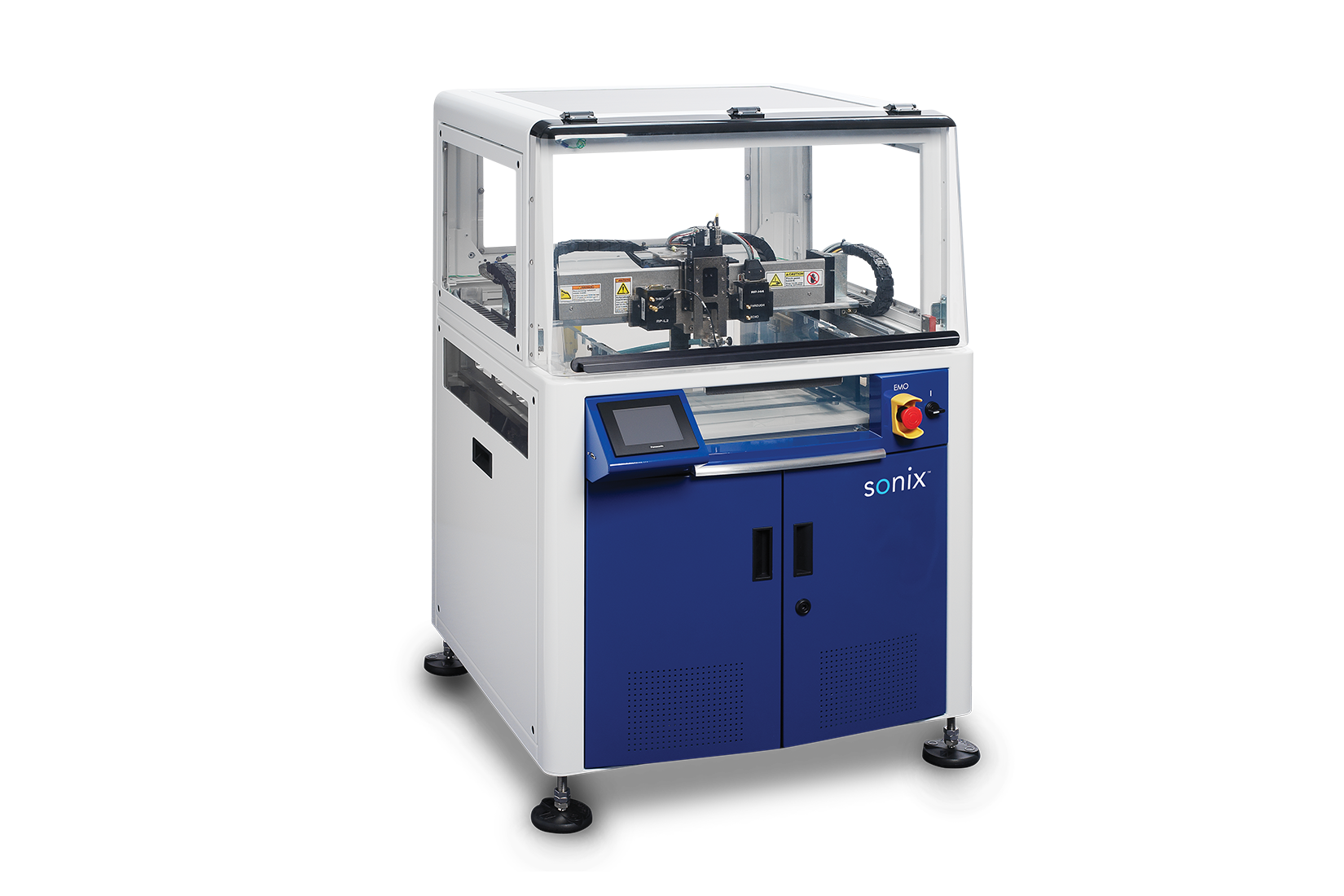
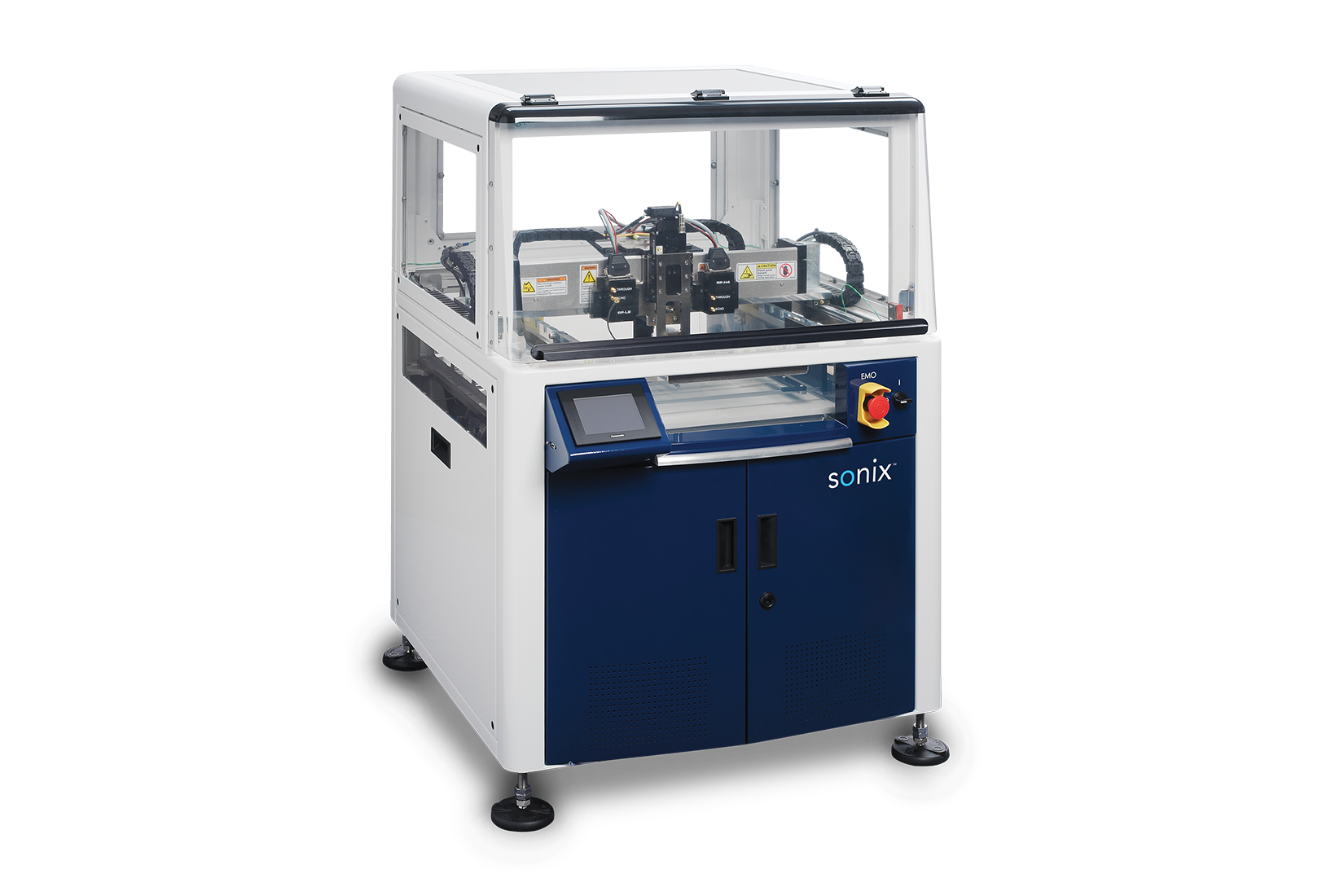
Stacked Die Package Inspection Features
Learn advanced inspection techniques for Cu Pillars, molded underfill and stacked die package. Download our new white paper.
© 2026 Sonix. All Rights Reserved.