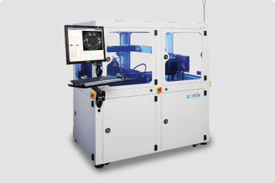
The ECHO scanning acoustic microscope is a nondestructive ultrasonic flaw detector designed to simplify testing, increase yield and maximize productivity in the lab or on the production floor.
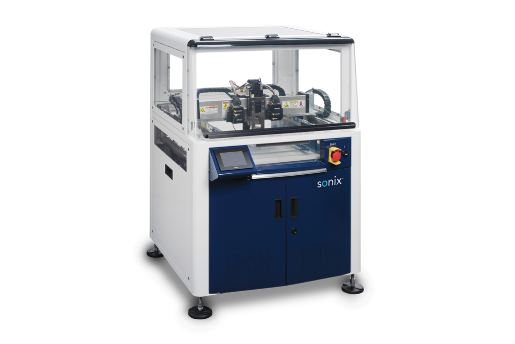
This industry-leading scanning acoustic microscope provides a universal inspection tool for packaged semiconductor development, production and failure analysis. With the ability to detect air defects as thin 0.05 micron and spatially resolve defects down to 10 microns, the ECHO is perfect for bump detection, stacked die (3D packaging) inspection, complex flip chip inspection and more traditional plastic packages.
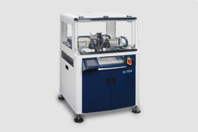
A robust, universal, ultrasonic flaw detector for overmolded single-die packages, bare flip chips and other standard applications
Sonix offers powerful wafer software tools to enhance bonded wafer imaging, accelerate production and adapt AutoWafer and AutoWafer Pro to our customers’ specific requirements.
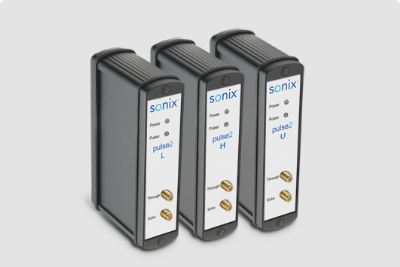
Sonix S-series ultrasonic NDT transducers are designed in-house to meet the demanding nondestructive testing requirements of semiconductor manufacturing. We offer the collaborative expertise to help customers choose the best ultrasonic NDT transducer for their application.

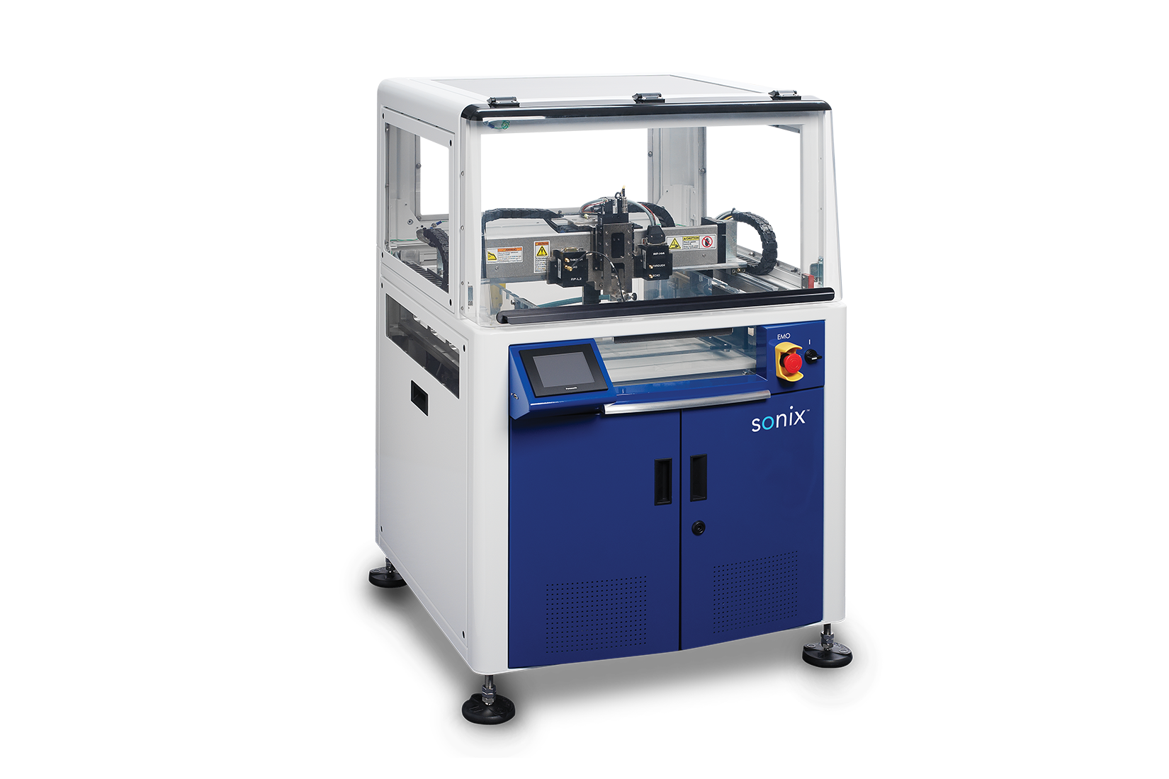
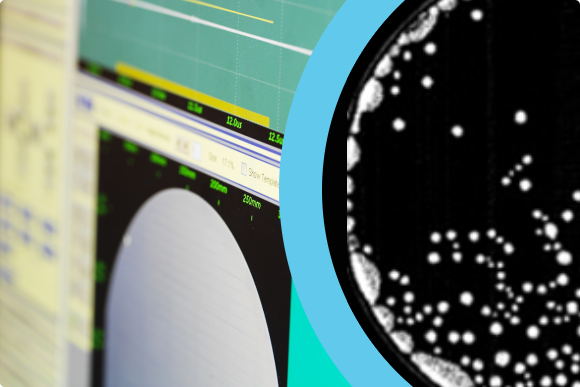
Sonix acoustic scanning microscopes offer precise IC inspection imaging for reliable defect detection and failure analysis

Provide a sample of your product. Sonix will provide you with an in-depth analysis report and help you develop an inspection solution designed to integrate into your process.
© 2026 Sonix. All Rights Reserved.