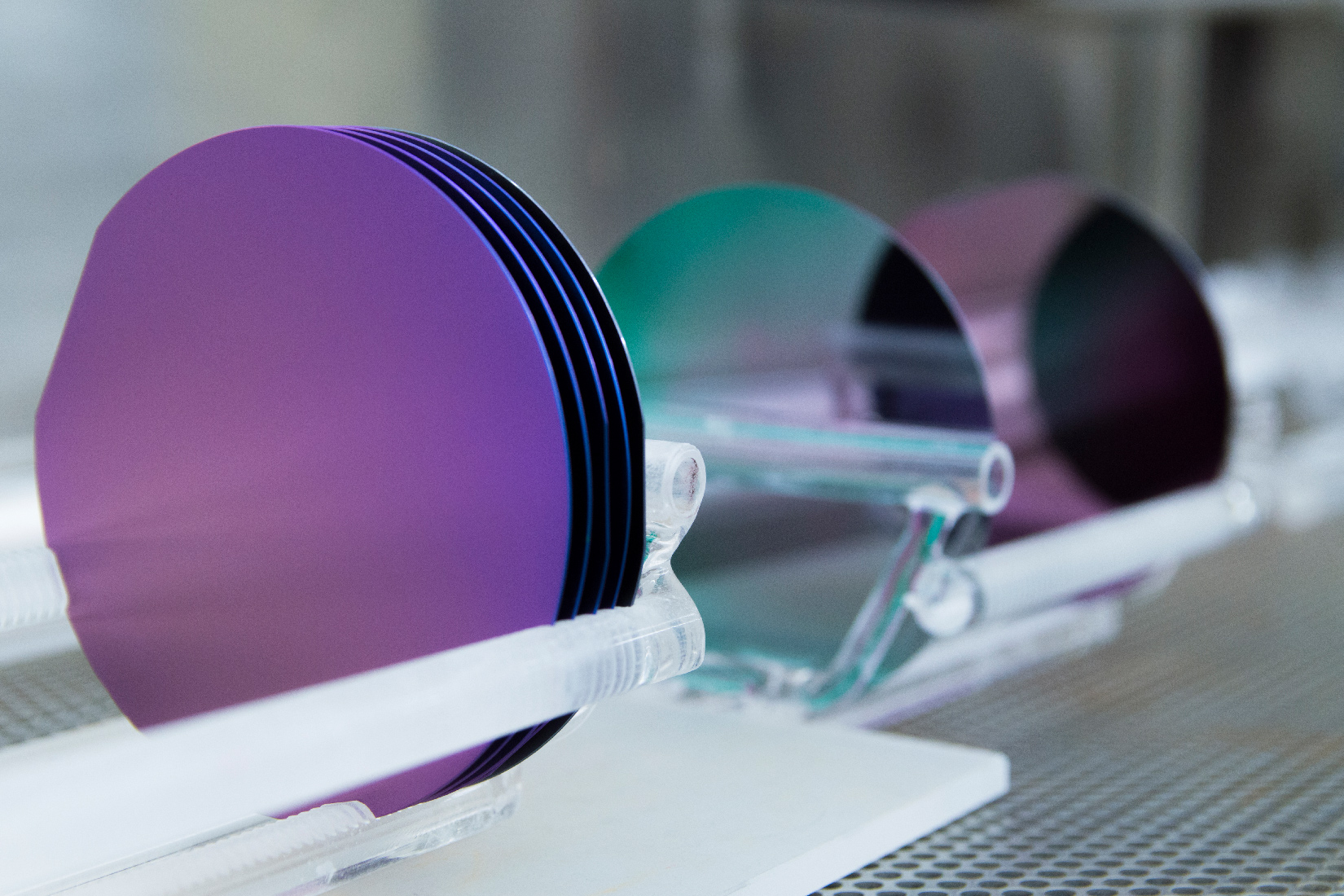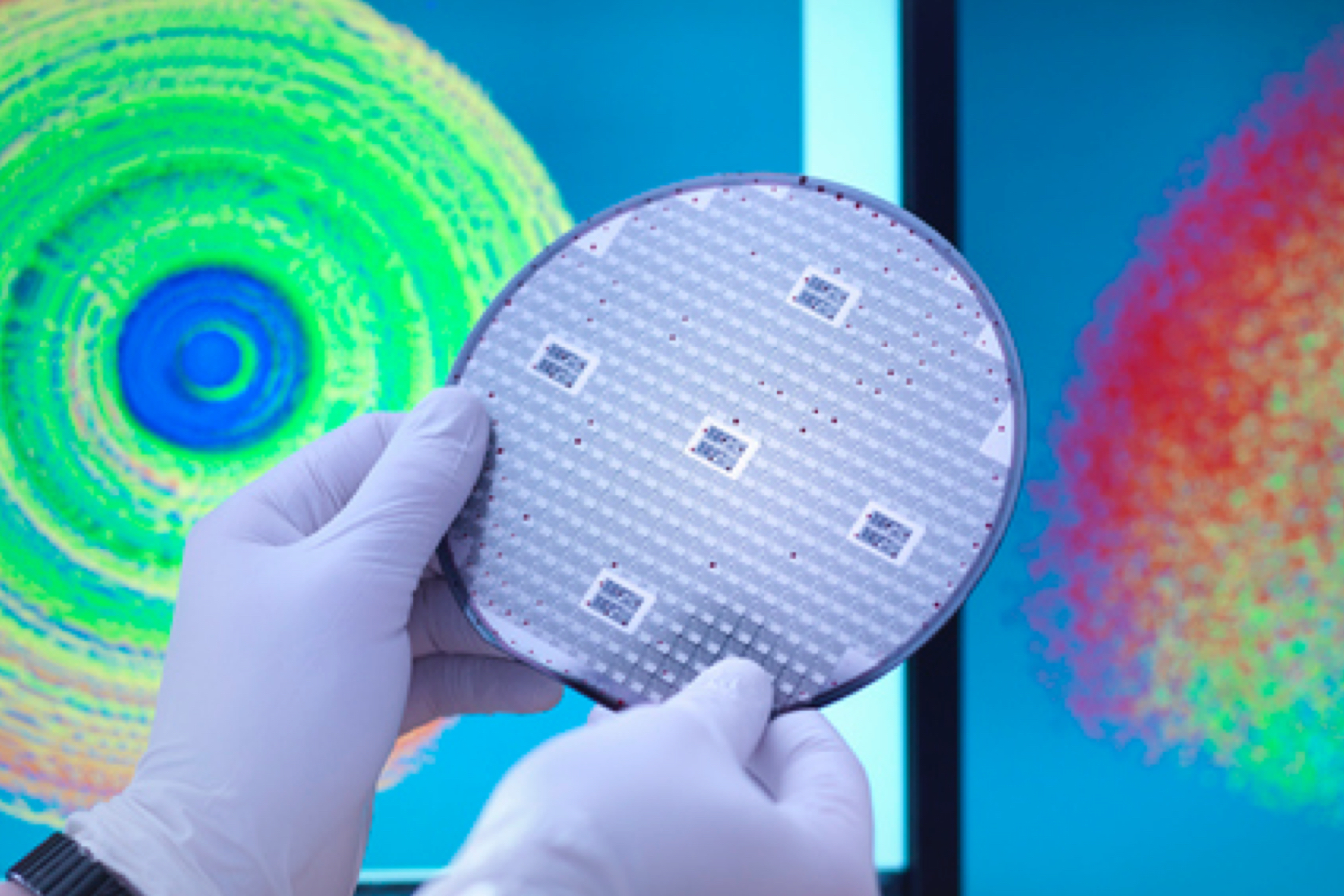
Relentless market demands for smaller, smarter products require a wafer solution that helps eliminate defects and improve yields from the very beginning of the fabrication process.
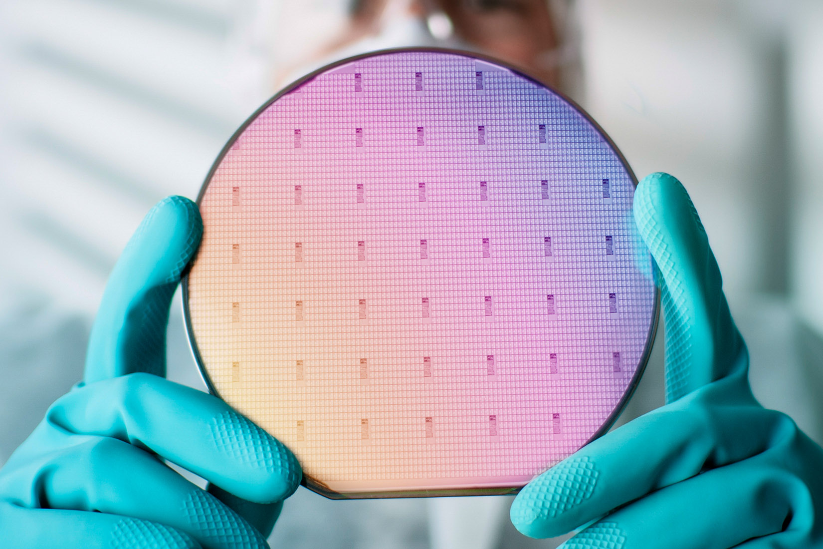
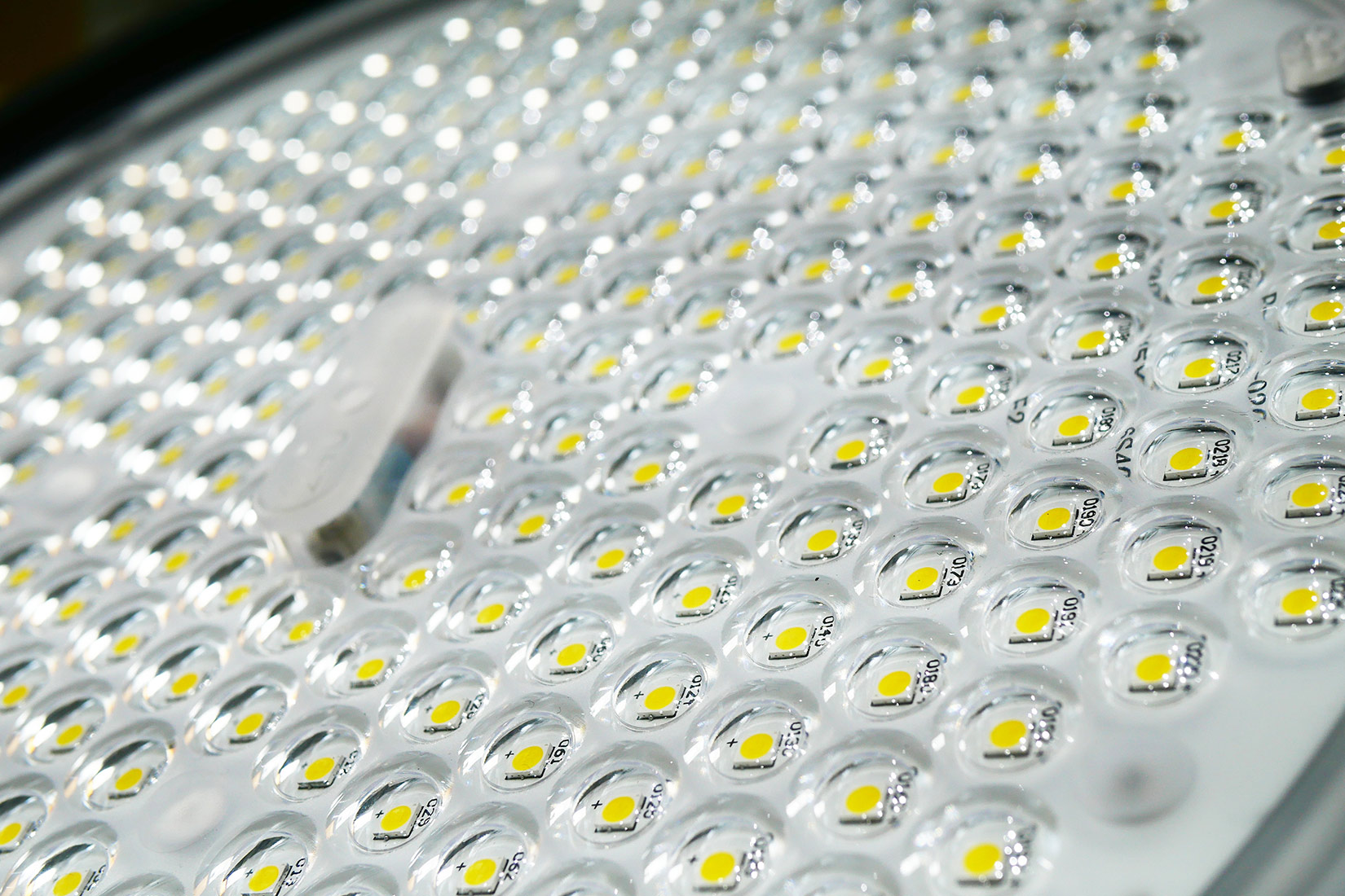
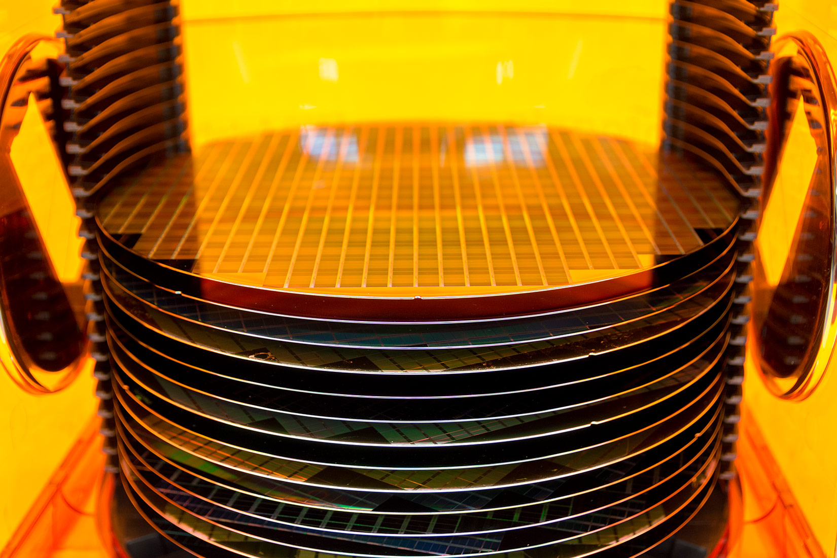
To meet a new market need, Sonix developed AutoWafer, the industry’s first wafer solution that enables fully automated inspection. With automated wafer processing and wafer analysis features, AutoWafer is optimized for production-speed inspection of MEMS, TSV, LED, BSI and other bonded wafer technologies.
© 2026 Sonix. All Rights Reserved.