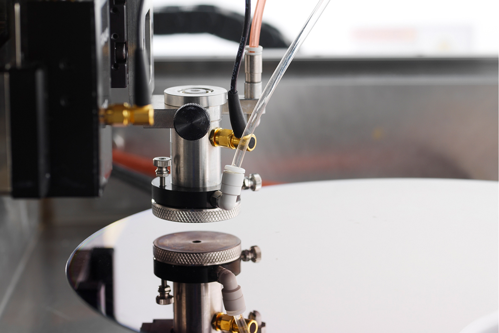
The backside illuminated sensor (BSI sensor) represents a major advancement in CMOS image sensor technology. BSI sensors allow compact cameras, phones and security systems to capture much more detailed images, even in low-light conditions, by eliminating the unnecessary reflectivity that occurs when the active matrix and its interconnects are located in front of the photocathode layer. To ensure the integrity of complex 3D bonds, nondestructive testing (NDT) of BSI sensors requires the ability to clearly inspect bonds in any position, at any depth in the bonded wafer. That’s where Sonix technology truly shines.
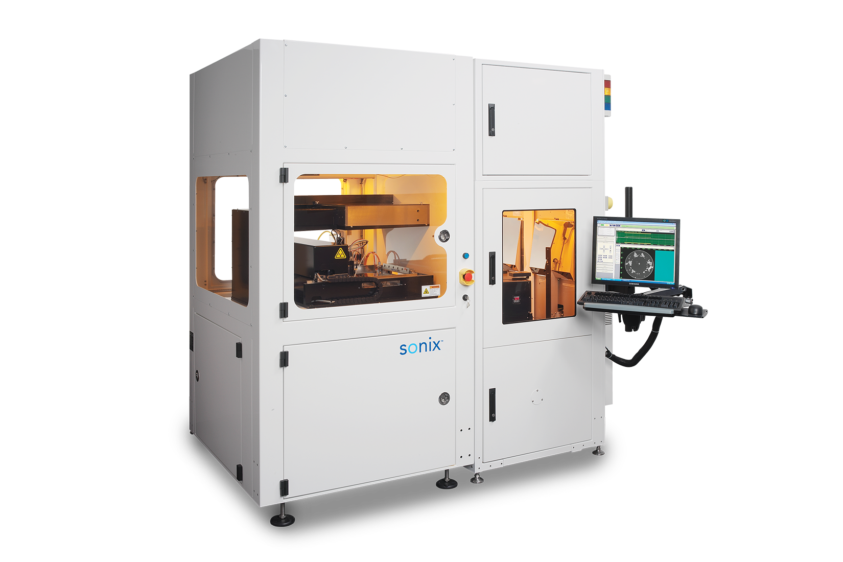
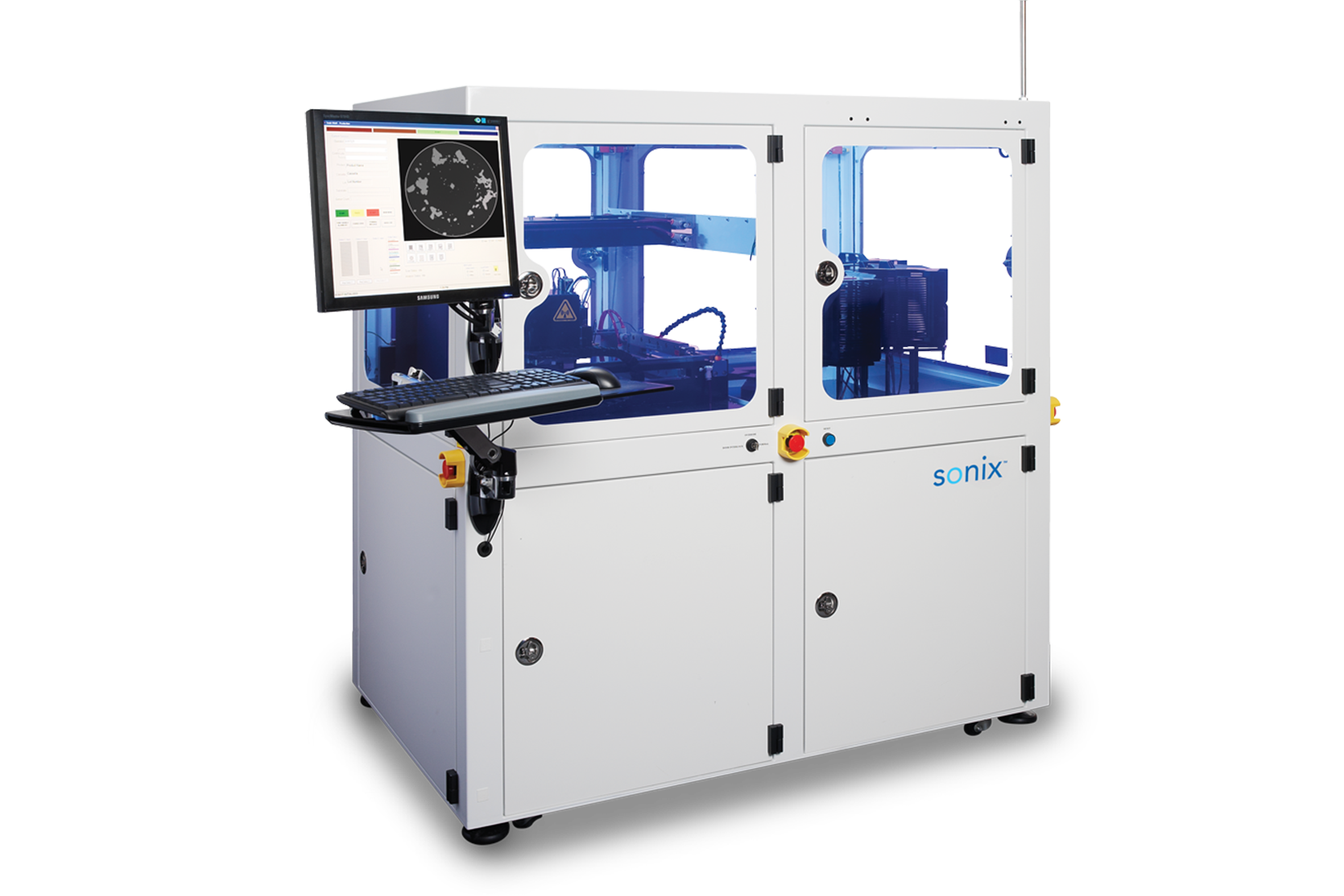
Sonix can help you choose the right transducers, designed in-house specifically for high-performance wafer inspection applications. Our pulse2 pulser/receiver substantially increases gain and signal-to-noise ratio for clear imaging at any depth, while our sophisticated analysis software helps you pinpoint regions of interest and interpret image data both qualitatively and quantitatively. In the production environment, NDT of backside illumination technology also requires efficient wafer handling to enable 100% inspection while meeting target yields. Sonix systems provide the image quality and analysis tools needed for advanced BSI sensor inspection, along with wafer-handling robotics designed to keep pace with high-throughput production.
BSI sensors were originally developed for specialized low-light applications such as security cameras, microscopes and telescopes. As costs come down, they are increasingly found in consumer still and video cameras, smartphones and other common products. To stay competitive, manufacturers are looking for more efficient ways to combine optics, memory and logic in the smallest possible space using advanced technologies such as stacked-die integration. Improved designs and manufacturing quality will continue to bring greater pixel density, light-capturing capability, reliability and affordability to a wide range of products – from mobile consumer devices to professional imaging equipment. Sonix image clarity and production throughput helps bring BSI technology innovation to light.
© 2026 Sonix. All Rights Reserved.