When manufacturing high-performance LEDs, it’s important to identify and remove defective LED dies from the manufacturing process before they reach the packaging stage. Efficient, accurate LED inspection and analysis at both the bonded LED wafer level and the LED die level is critical to maximizing product reliability and profitability, as well as improving manufacturing processes to improve yields.
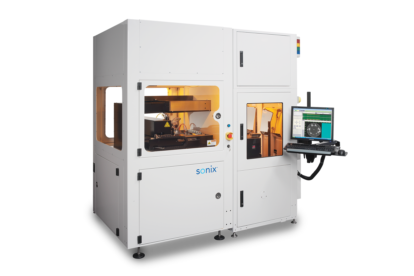
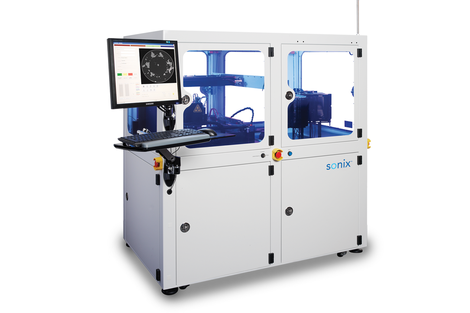
Reliable Analysis of Wafer- and Device-Level Defects at Production Speeds
Sonix automated wafer inspection systems provide superior image quality, with a complete range of transducers designed in-house to provide optimum penetration and resolution for your application. Our Flexible TAMI™ software enables the control and speed to allow both multilayer wafer- and device-level analysis of LED dies in a single scan. The Sonix pulse2 pulser/receiver improves signal-to-noise ratio and gain for clean, clear imaging at any frequency and depth. Our image analysis software supports quantitative and qualitative interpretation of image data, including an automated analysis option for the production environment. And our exclusive wafer handling and drying processes support the highest LED inspection throughput on your production line, with minimal operator intervention.
Sonix for any LED Application
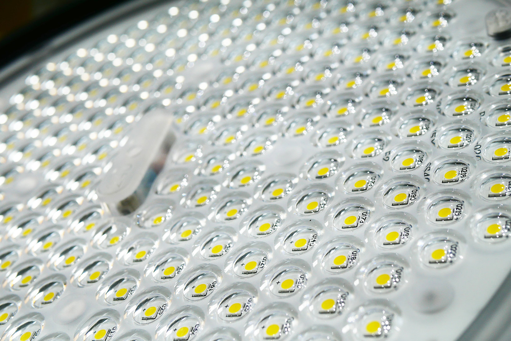
In a few short years, LEDs have gone far beyond the realm of low-power indicator and signaling lamps to achieve widespread adoption in lighting applications ranging from general-purpose indoor and outdoor fixtures to architectural luminaires, industrial systems, floodlights and decorative lights. LEDs are also bringing new capabilities to applications such as backlit displays, DLP projectors, medical devices, communications systems, sensor systems and more. And the LED revolution is just beginning. Prototypes for LED-based augmented reality contact lenses, interactive wallpaper and “virtual sky” lighting have already been developed, to cite just a few examples. As greater LED power and miniaturization enable previously unimaginable applications, manufacturers will need the ability to detect defects at the smallest sizes, in the largest production quantities, at the highest speeds. Sonix lights a clear path to the future.
© 2026 Sonix. All Rights Reserved.