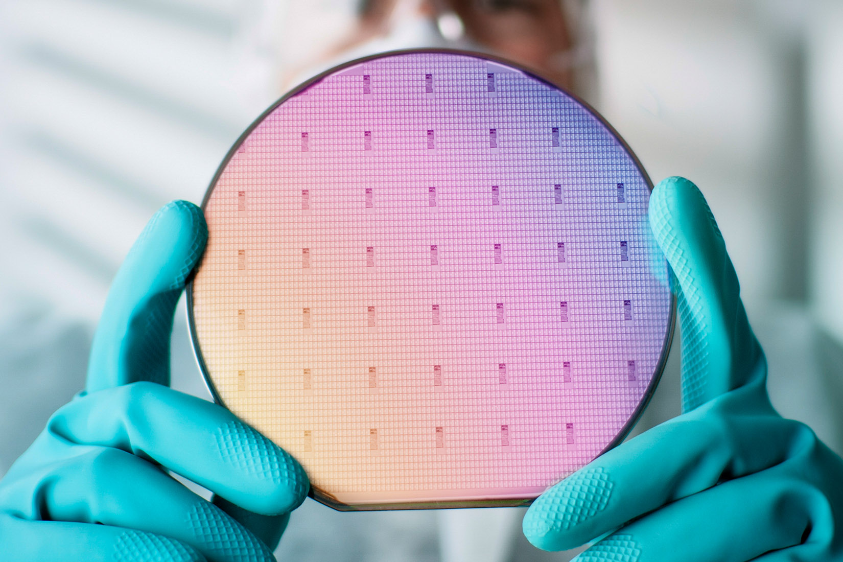
Microelectromechanical systems (MEMS) allow equipment such as pressure sensors, microphones, gyroscopes and accelerometers to be incorporated in silicon devices. Because MEMS technology structures are so small and delicate, they depend on the integrity of the hermetic bond to avoid contamination and ensure reliable operation. Nondestructive testing (NDT) for MEMS applications in a production environment depends on clear imaging of every critical bond ring on every device. In MEMS applications for deploying automotive airbags, for example, 100% MEMS inspection is required to comply with safety regulations. In a motion-sensitive smartphone application, 100% MEMS inspection helps avoid warranty costs and ensure customer satisfaction. That’s why Sonix is with you 100%.
Clear Imaging and Analysis at Production Speeds
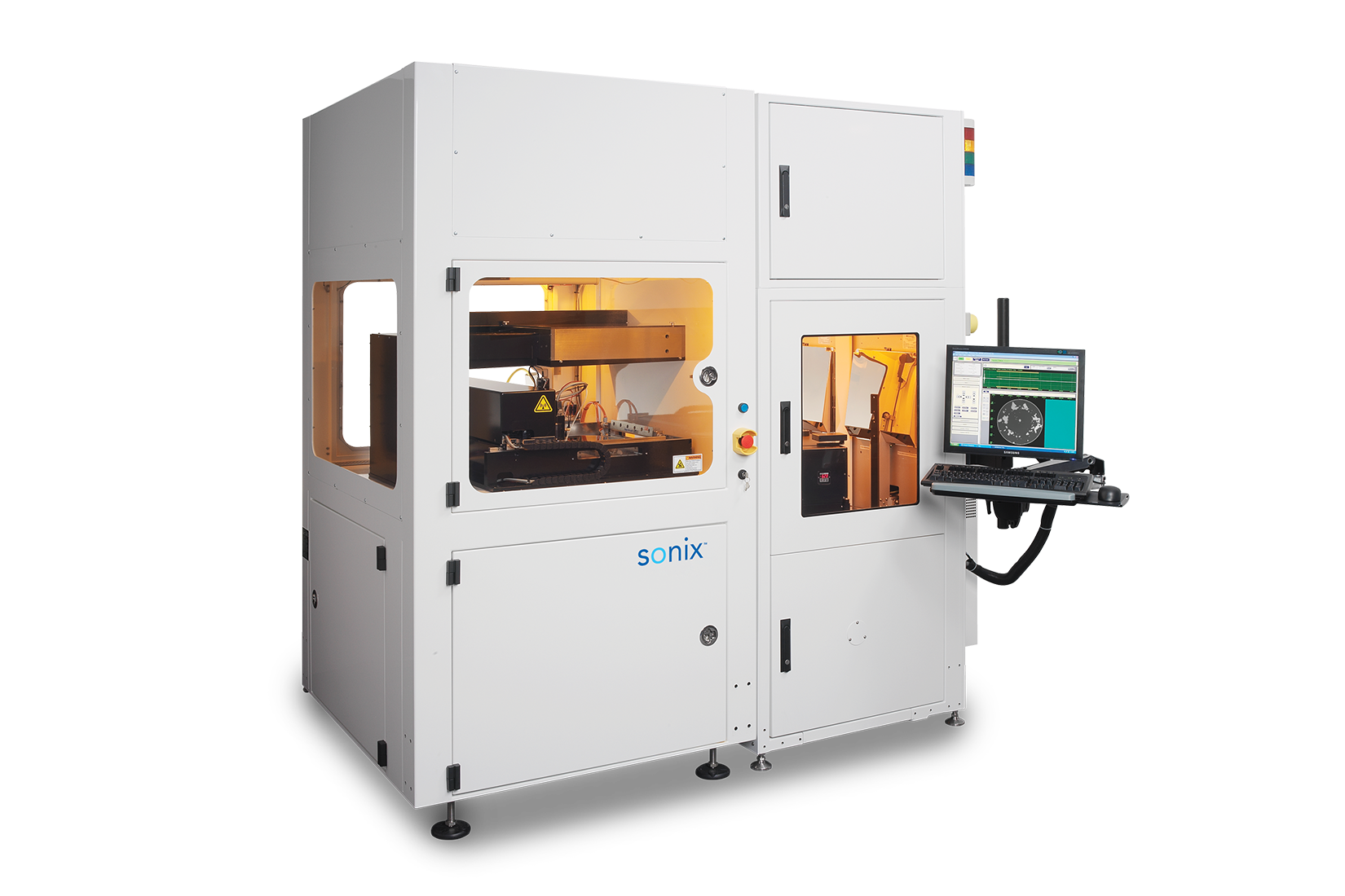
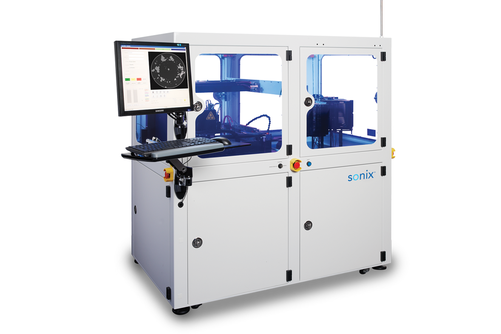
Sonix wafer inspection systems provide the image quality and throughput needed for 100% inspection in the most challenging MEMS applications. Our AutoWafer™ and AutoWafer Pro™ systems offer high-resolution scanning and production-speed throughput, with automated handling and sorting of approved and failed wafers. Our complete selection of transducers, designed in-house, optimize spatial and depth resolution to provide the clearest imaging for your application. Our pulse2 pulser/receiver improves signal quality and resolution for clear imaging of the smallest defects. And we offer the industry’s most sophisticated software for defining regions of interest, distinguishing bond line defects from MEMS cavities, and analyzing scan results.
Sonix for any MEMS Application
MEMS devices – such as microphones, pressure sensors, accelerometers, gyroscopes, optical switches, microactuators and microscanners – bring sophisticated sensing and control capabilities to a growing range of applications. These remarkable miniature sensors are transforming automobiles, biotech systems and medical devices, mobile phones and tablets, communications systems and many other current and future applications. As MEMS devices become an ubiquitous part of everyday life, manufacturers need a reliable partner for nondestructive inspection to assure quality in product development and production. That partner is Sonix.
© 2026 Sonix. All Rights Reserved.