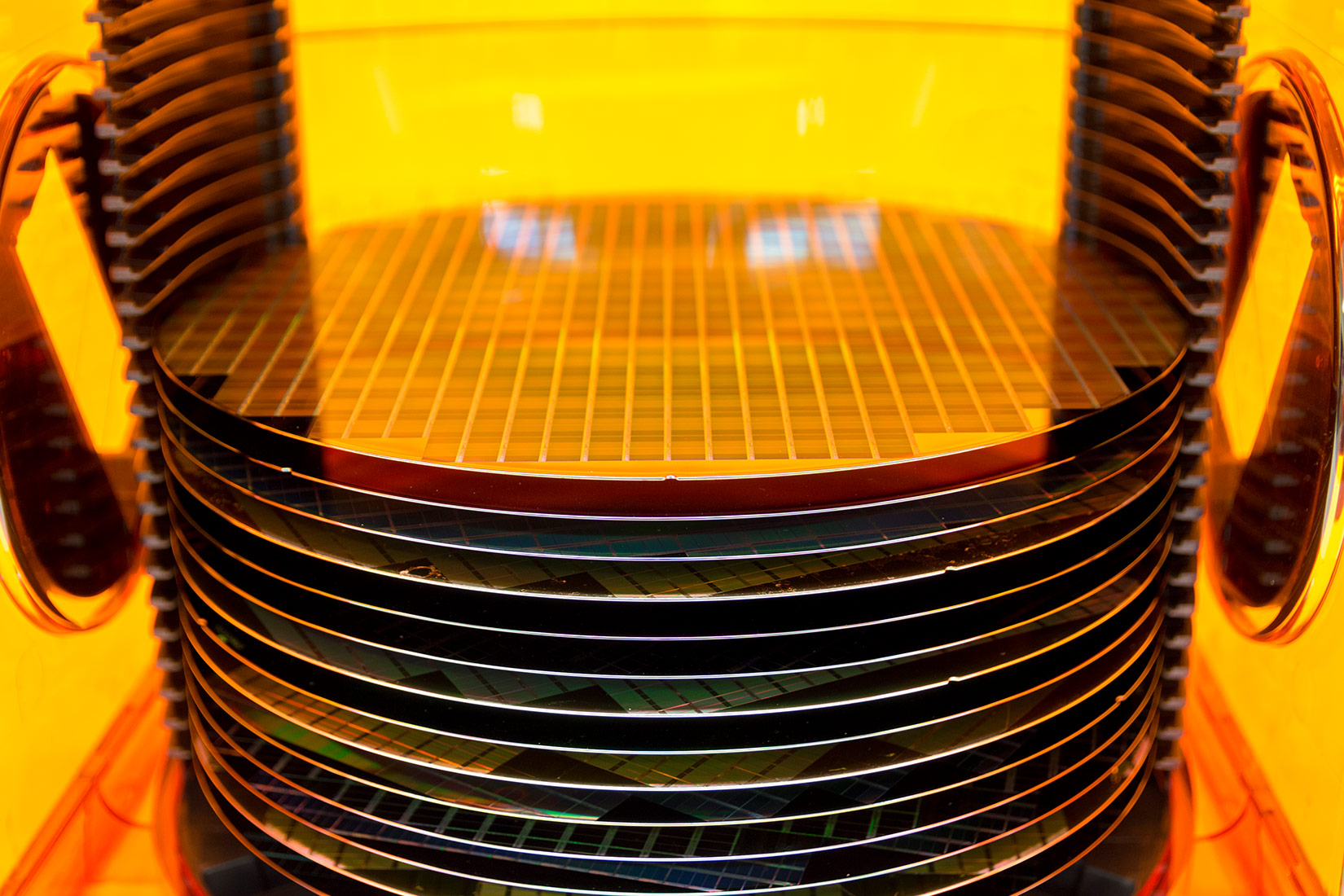
The need for increased functionality and speed in a smaller footprint has led manufacturers to stacked die solutions, with TSV (through-silicon via) technology providing electrical connections between device layers. To help ensure reliable operation, TSV inspection verifies that the holes and trenches containing through-silicon vias have the proper depth, width and uniformity and that the TSV conductors within them are free of voids and cracks. Because through-silicon vias are structured in the z-dimension, TSV inspection and analysis can be particularly challenging. Sonix is up for any challenge.
A Clear View of Three-Dimensional Features
Sonix systems provide advanced wafer metrology features to enable high-resolution TSV inspection of well-defined regions of interest, efficiently gathering data in all directions in a single scan. Our transducers are designed in-house to provide the penetration, focus and resolution required to clearly detect cracks, voids and misalignments in these microscopic 3D interconnects. To generate the highest quality signal, our pulse2 pulser/receiver provides 12 dB of extra gain and a fourfold improvement in signal-to-noise ratio. We also offer the industry’s most advanced defect analysis and metrology software, including tools to measure the depth and width of a line of trenches and TSVs across a time-of-flight image.
Sonix for any TSV Application
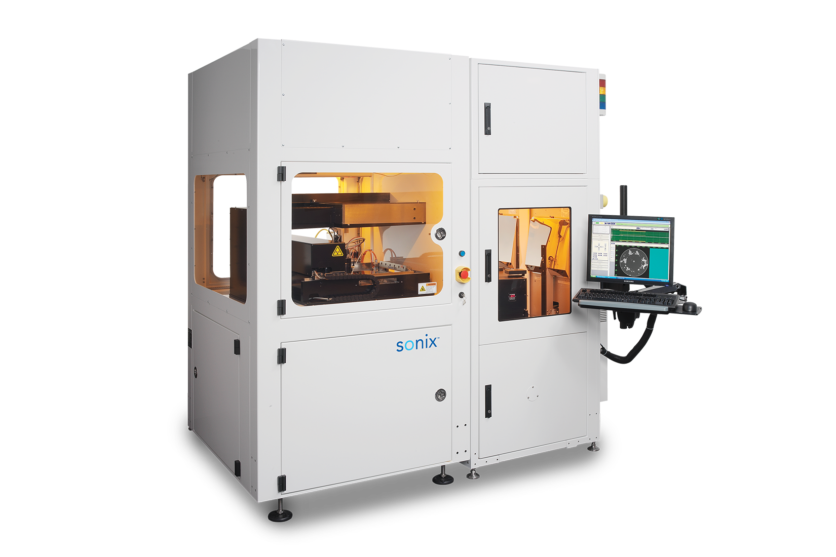
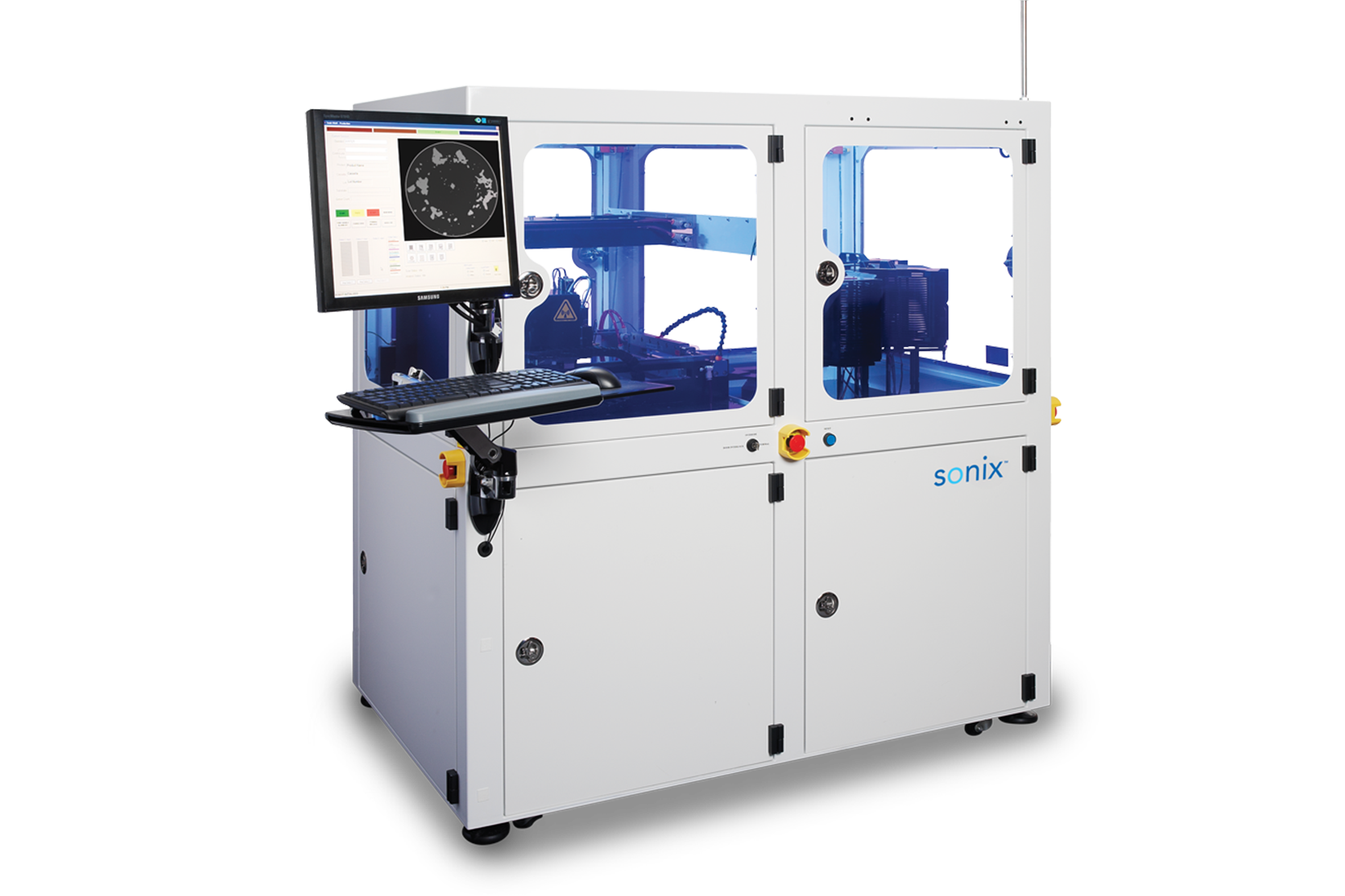
The classic use for TSVs is in backside illuminated (BSI) CMOS image sensors, improving image capture in low-light conditions by enabling the active matrix and its interconnects to be placed behind the photocathode layer. However, TSVs provide many more benefits – eliminating the need for wire bonds, enabling shorter and faster interconnects, increasing interconnect density and, most important, enabling 3D stacking of circuits to offer more functionality, memory and processing power in a smaller footprint. For these reasons, TSVs are increasingly being used to enable the most sophisticated applications, such as 3D chip-stack and system-in-package devices for smartphones and other space-constrained mobile devices. All of these applications depend on ensuring TSV quality during bonded wafer manufacturing. Sonix AutoWafer™ and AutoWafer Pro™ systems deliver quality assurance for TSVs at full production speeds.
© 2026 Sonix. All Rights Reserved.