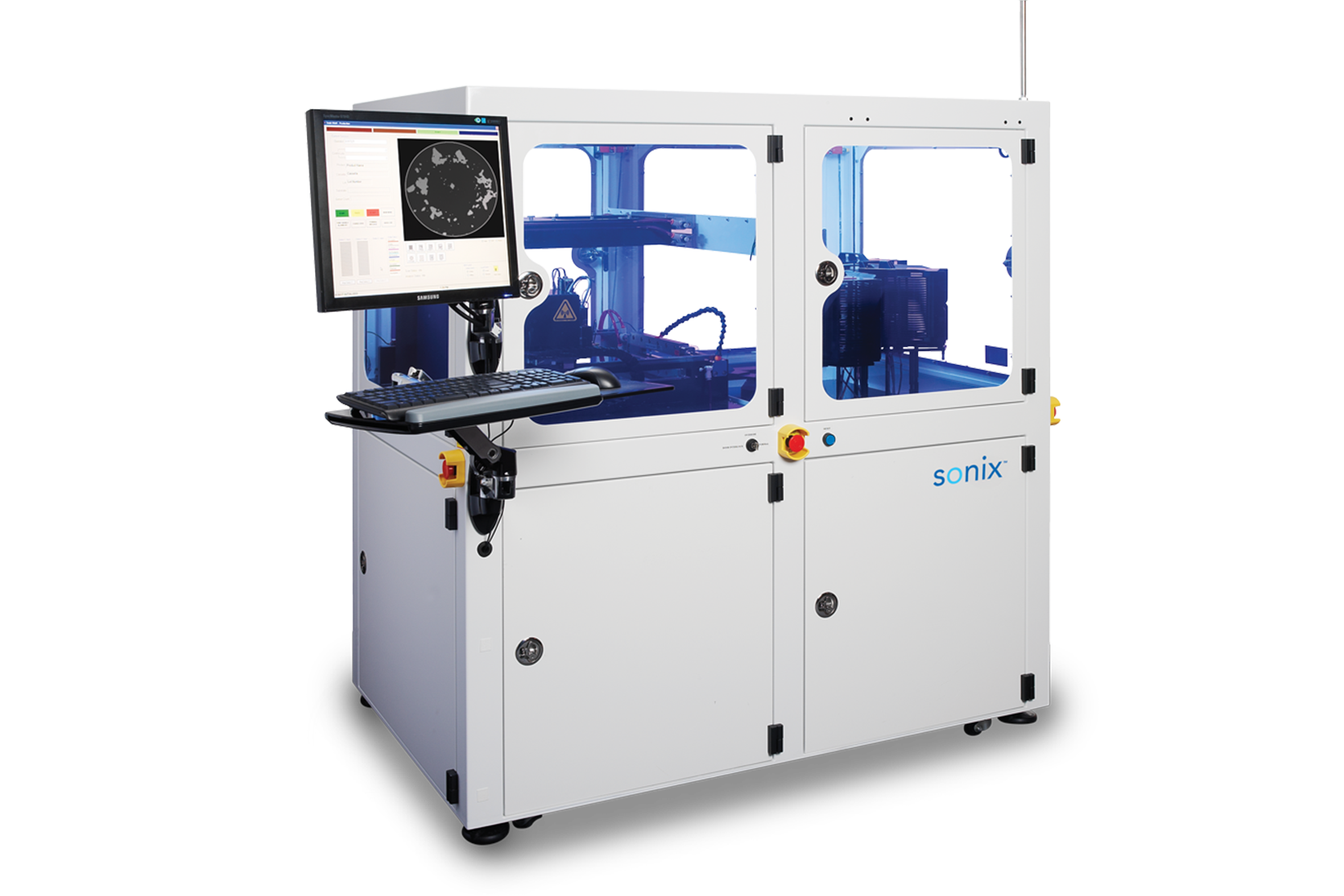
AutoWafer pro is our most advanced ultrasonic equipment for detecting defects in bonded wafers in a production environment, providing fast, high-resolution scanning of 200mm and 300mm bonded wafers.
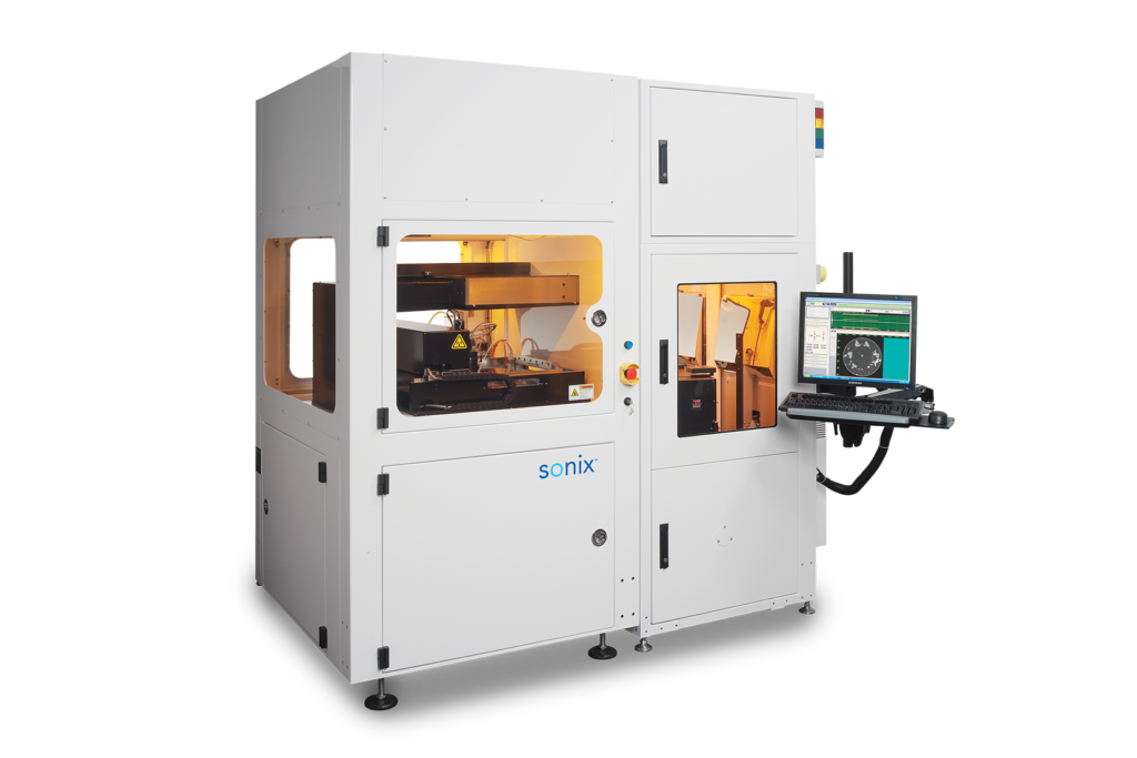
A flexible, automated wafer inspection system designed for production, AutoWafer Pro provides fast, high-resolution scanning of 200mm and 300mm bonded wafers. It’s the ideal ultrasonic equipment for identifying bond defects in wafer applications such as MEMS, BSI Sensors, CMOS, memory, TSV and LED.
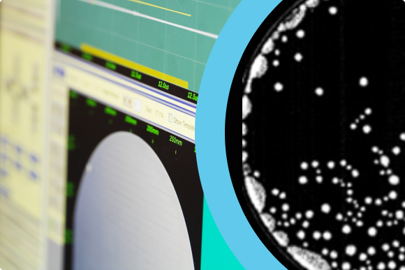
With extensive analysis capabilities at both the wafer and device level, there’s no need to reload and rescan wafers to get all the diagnostic images you need. And with high-speed scanning managed by fully automated wafer handling, AutoWafer Pro supports 100% nondestructive testing (NDT) for improved yields and a faster time to market.
Sonix offers powerful wafer software tools to enhance bonded wafer imaging, accelerate production and adapt AutoWafer and AutoWafer Pro to our customers’ specific requirements.
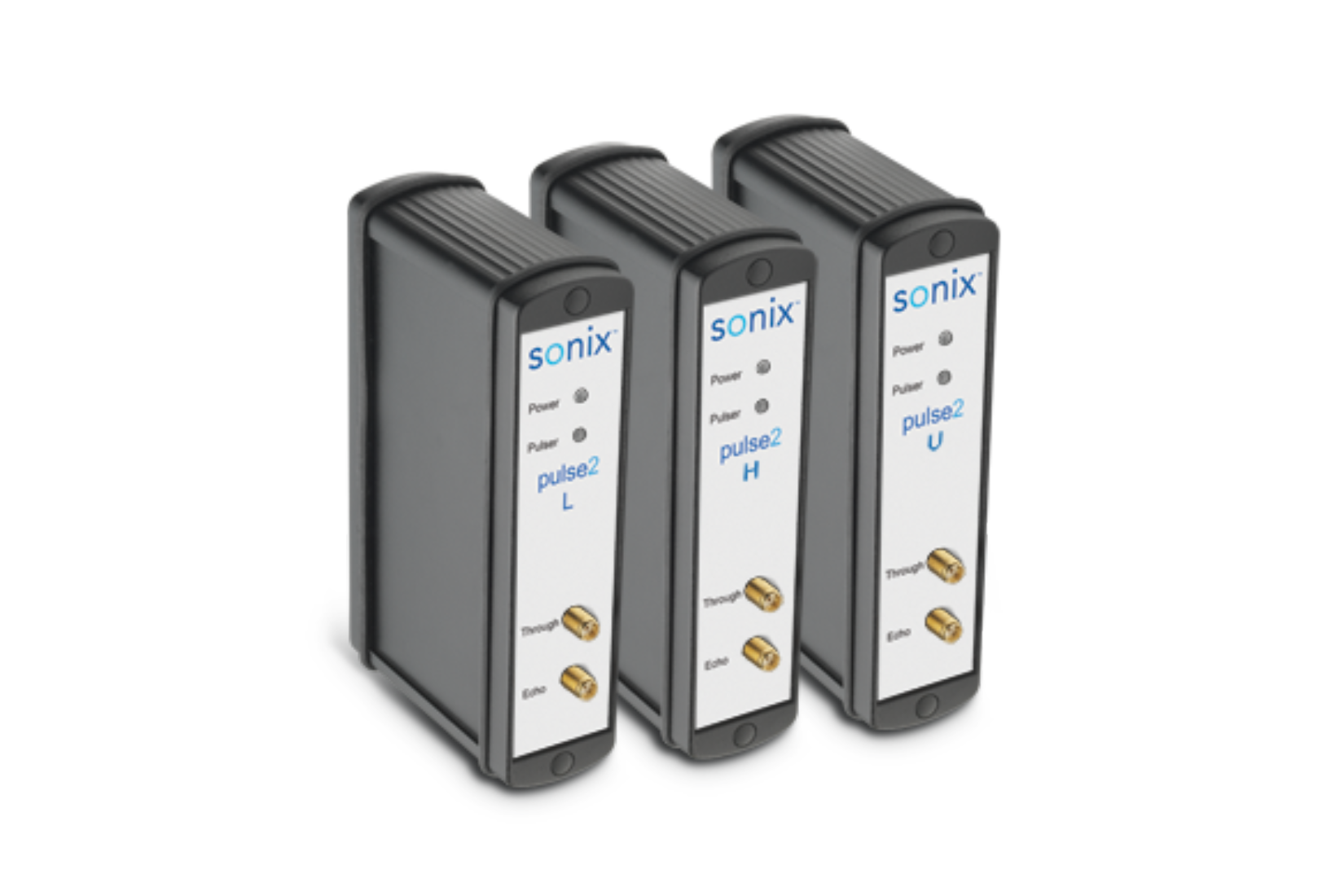
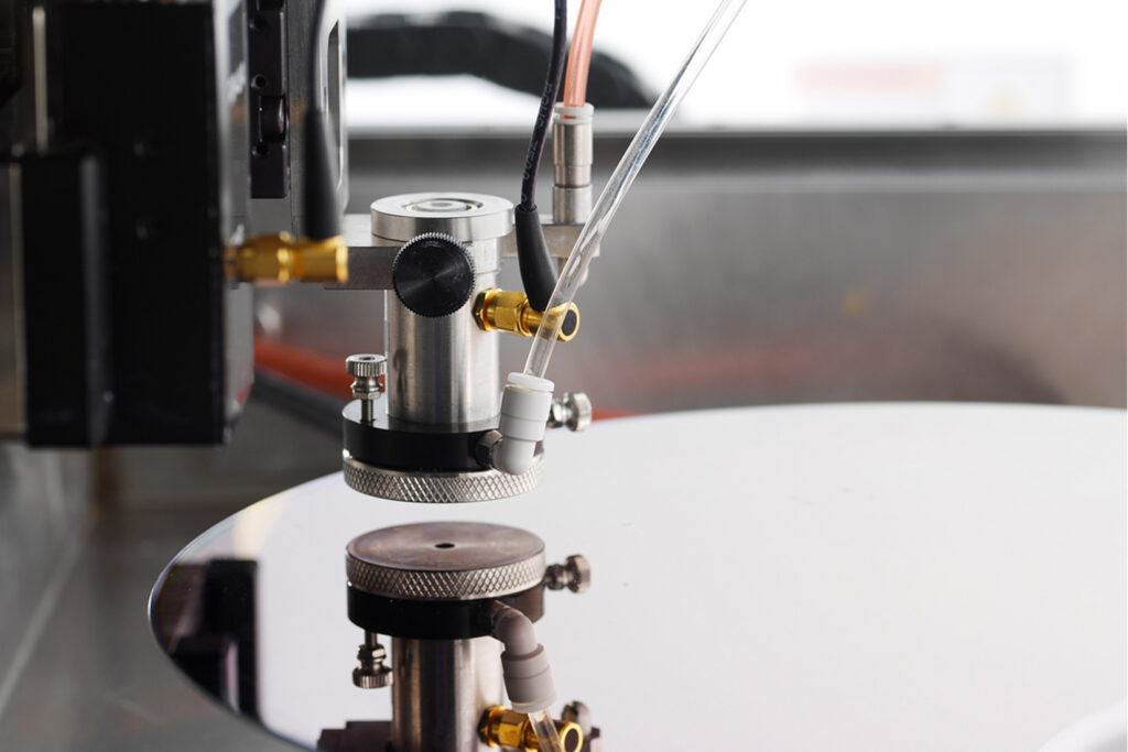
Sonix S-series ultrasonic NDT transducers are designed in-house to meet the demanding nondestructive testing requirements of semiconductor manufacturing. We offer the collaborative expertise to help customers choose the best ultrasonic NDT transducer for their application.
BSI sensors allow compact cameras, phones and security systems to capture much more detailed images, even in low-light conditions, by eliminating the unnecessary reflectivity that occurs when the active matrix and its interconnects are located in front of the photocathode layer.

Provide a sample of your product. Sonix will provide you with an in-depth analysis report and help you develop an inspection solution designed to integrate into your process.
© 2026 Sonix. All Rights Reserved.