Since 1986, Sonix has pioneered many of the breakthroughs in defect detection and process productivity that have helped semiconductor manufacturers create a world of new possibilities.
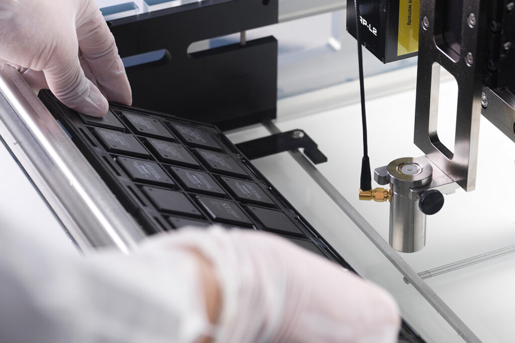
Today, manufacturers around the world depend on our scanning acoustic microscope technology for nondestructive inspection of bonded wafers, packaged semiconductors, and industrial products. And we continue to lead the way with new ultrasonic technologies and applications to assure the quality of tomorrow’s innovations.

Where other have failed, we have consistently found the right answers to very difficult problems. Today, Sonix acoustic scanning microscopes are used by leading manufacturers worldwide to perform nondestructive inspection of bonded wafers and packaged semiconductors, from the development lab to the production floor.
Find out about our history, partnerships, global presence, and more.
Looking for answers? If you don’t see what you need here, contact our support team with any product question or technical issue.
© 2025 Sonix. All Rights Reserved.