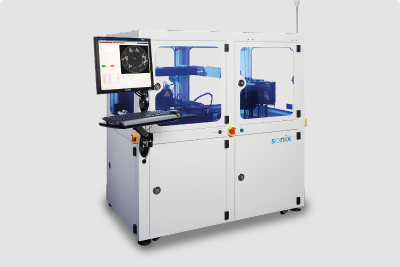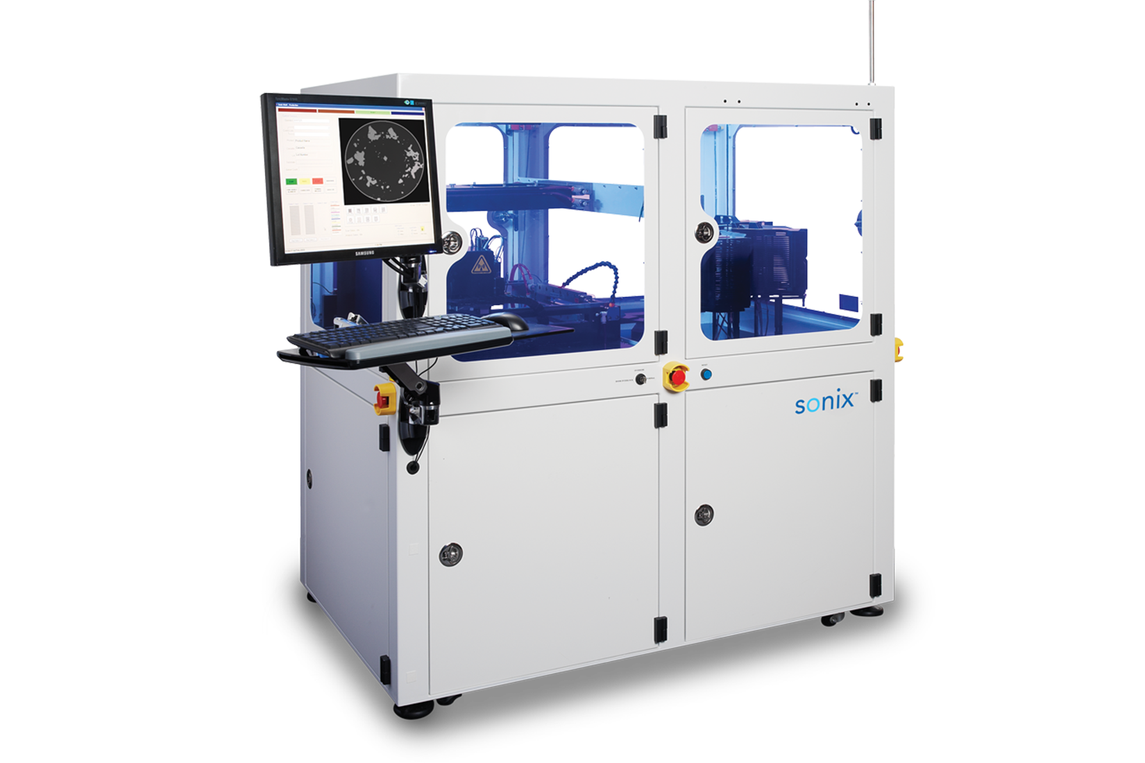
Installed in more wafer applications than all other automatic ultrasonic testing tools combined, AutoWafer provides a complete, production-ready wafer scanner for wafers from 100mm to 200mm, including multiple sizes in a single batch.
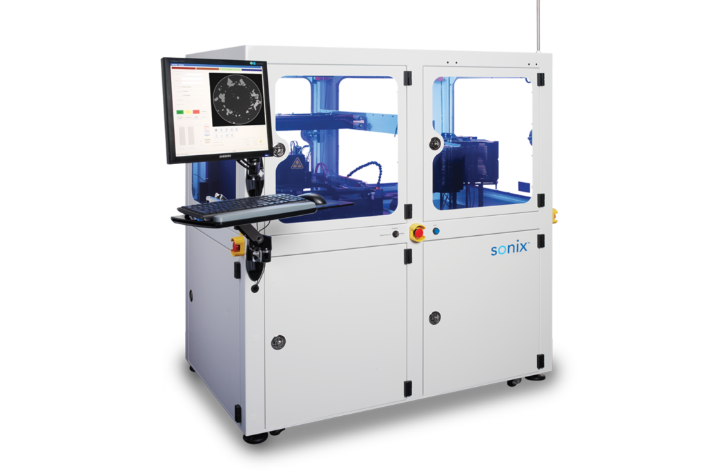
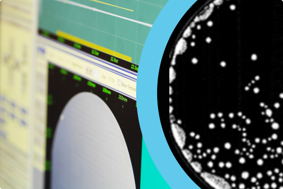
AutoWafer is an ultrasonic wafer scanner for nondestructive testing (NDT) of wafers in development and production environments, providing high-resolution identification of bond defects in wafer applications such as MEMS, CMOS, memory, TSV and LED. Robotic cassette handling and sorting of approved and failed wafers helps speed production, while our advanced transducers and auto-analysis tools make it quick and easy to identify even the smallest, most subtle defects.
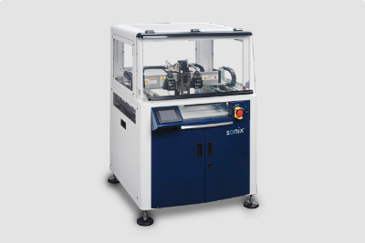
Sonix offers powerful wafer software tools to enhance bonded wafer imaging, accelerate production and adapt AutoWafer and AutoWafer Pro to our customers’ specific requirements.
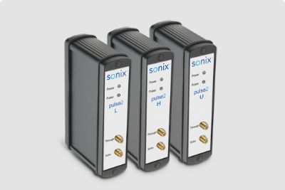
Sonix S-series ultrasonic NDT transducers are designed in-house to meet the demanding nondestructive testing requirements of semiconductor manufacturing. We offer the collaborative expertise to help customers choose the best ultrasonic NDT transducer for their application.
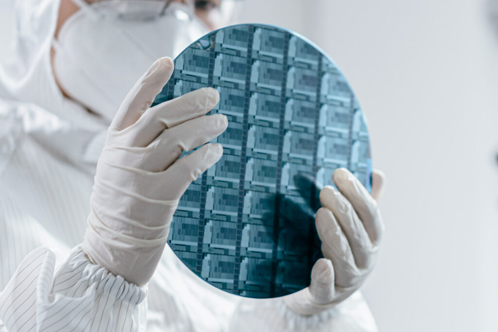
Microelectromechanical systems (MEMS) allow equipment such as pressure sensors, microphones, gyroscopes and accelerometers to be incorporated in silicon devices.

Provide a sample of your product. Sonix will provide you with an in-depth analysis report and help you develop an inspection solution designed to integrate into your process.
© 2026 Sonix. All Rights Reserved.